XCV200E-6FG256C Device Overview and Functional Structure
Working with programmable hardware becomes easier when you understand how a device like the XCV200E-6FG256C operates inside a system. You can use it to create custom digital logic, manage signals, and connect different parts of electronic equipment through configurable circuits. Its programmable structure allows you to define logic behavior through configuration data rather than fixed wiring. With built-in memory, structured logic blocks, and many input and output connections, you get a flexible platform that supports control logic, signal handling, and communication functions within compact electronic designs.Catalog
XCV200E-6FG256C Overview
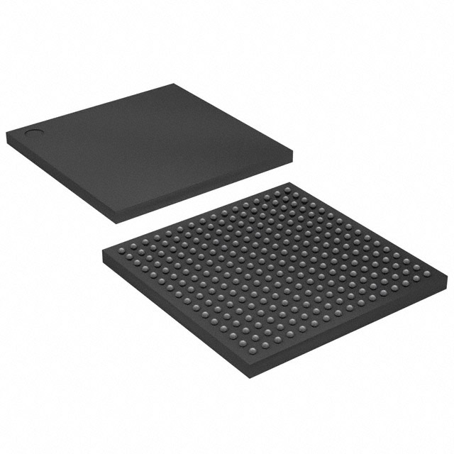
The XCV200E-6FG256C is a programmable logic device used to build custom digital functions inside electronic systems. It belongs to the Virtex-E FPGA family and integrates programmable logic cells, internal memory blocks, and routing paths that allow digital circuits to be defined through configuration data. The device provides 176 input and output connections and supports more than three hundred thousand logic gates for implementing control logic, data processing paths, and interface management. Operating from a 1.71 V to 1.89 V supply range, it uses a 256-ball FBGA package designed for surface mounted circuit boards in compact electronic equipment.
Looking for XCV200E-6FG256C? Contact us to check current stock, lead time, and pricing.
Banks of XCV200E-6FG256C
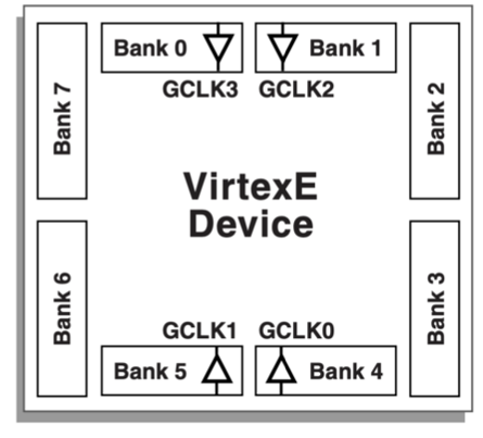
Input and output resources of the XCV200E-6FG256C are divided into eight separate banks arranged around the perimeter of the device to organize external signal connections. Each bank groups multiple Input Output Blocks that share common voltage and configuration settings for interface compatibility. Banks labeled 0 through 7 are positioned along the four sides of the device, forming the boundary between the internal programmable logic and the external package pins. Four global clock inputs labeled GCLK0, GCLK1, GCLK2, and GCLK3 are distributed across these banks to deliver clock signals into the internal routing network. This banked structure allows different signaling standards to operate in separate regions while maintaining consistent electrical behavior within each bank.
XCV200E-6FG256C CAD Model
XCV200E-6FG256C Symbol
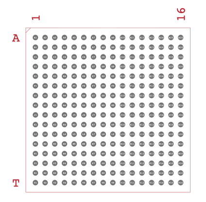
XCV200E-6FG256C Footprint
XCV200E-6FG256C 3D Model
Features of XCV200E-6FG256C
Programmable Logic Fabric
The device contains a structured array of configurable logic blocks arranged across the chip to create digital circuits through programmable connections. Each block can implement combinational logic, small storage elements, and control functions, allowing designers to define custom digital behavior inside one component.
Embedded Block Memory
Integrated memory blocks provide internal storage that supports buffering, lookup tables, and temporary data handling during operation. These memory resources reduce the need for external memory devices and allow data processing tasks to occur directly inside the programmable logic structure.
High I O Connectivity
Up to 176 input and output connections are available to link the programmable logic with external components. These connections are arranged in organized banks, which allows the device to communicate with multiple system interfaces while maintaining consistent signal behavior across each bank.
Global Clock Distribution
Dedicated clock input paths distribute timing signals across the device through controlled routing channels. This arrangement keeps clock signals aligned across logic regions, helping sequential circuits operate in step with the system timing reference.
Internal Routing Network
An internal network of programmable interconnect lines links logic blocks, memory elements, and input output structures. These routing resources allow signals to travel between functional areas of the device and support flexible digital circuit layouts.
Surface Mount FBGA Package
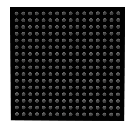
The device uses a 256 ball fine pitch ball grid array package designed for surface mount assembly. This format supports compact circuit board layouts while providing the electrical connections required for logic signals, power distribution, and control lines.
Stable Supply Voltage Operation
Operation within a 1.71 V to 1.89 V supply range supports stable electrical behavior during system activity. This voltage range is suitable for programmable logic devices that integrate multiple functional blocks within a single silicon structure.
XCV200E-6FG256C Technical Specifications
| Product Attribute | Attribute Value |
| Manufacturer | AMD Xilinx |
| Voltage - Supply | 1.71V ~ 1.89V |
| Total RAM Bits | 114688 |
| Supplier Device Package | 256-FBGA (17x17) |
| Series | Virtex®-E |
| Package / Case | 256-BGA |
| Package | Tray |
| Operating Temperature | 0°C ~ 85°C (TJ) |
| Number of Logic Elements/Cells | 5292 |
| Number of LABs/CLBs | 1176 |
| Number of I/O | 176 |
| Number of Gates | 306393 |
| Mounting Type | Surface Mount |
| Base Product Number | XCV200E |
| RoHS Status | RoHS non-compliant |
| Moisture Sensitivity Level (MSL) | 3 (168 Hours) |
| REACH Status | REACH Unaffected |
| ECCN | 3A001A7B |
| HTSUS | 8542.39.0001 |
Architecture Overview of XCV200E-6FG256C
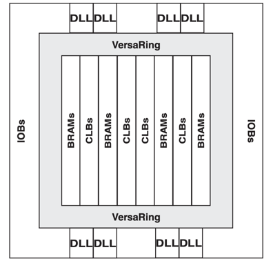
Central logic fabric arranged as vertical columns of Configurable Logic Blocks labeled CLBs forms the programmable core used to implement digital logic functions inside the XCV200E-6FG256C. Dedicated memory columns labeled BRAMs are distributed among the logic columns and provide embedded storage for data buffering and internal processing tasks. A routing structure labeled VersaRing surrounds the core region and provides additional signal paths that connect the logic array with the outer interface resources. Input and Output Blocks labeled IOBs line the outer perimeter of the device and connect the internal logic network to external pins of the package. Clock management resources labeled DLL are positioned along the edges of the architecture and support controlled distribution of clock signals across the programmable logic structure.
Input Output Block of XCV200E-6FG256C
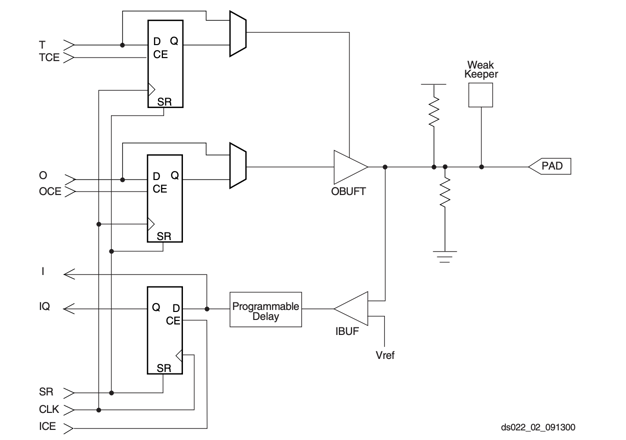
Internal input and output structure organized around a central pad connection defines how signals enter and leave the XCV200E-6FG256C device. Output data passes through a configurable flip flop stage with clock enable and set reset control before reaching a tri state output buffer labeled OBUFT that drives the external pad. Input signals arriving from the pad are routed through an input buffer labeled IBUF and can pass through a programmable delay stage before reaching internal logic registers. Additional control signals including clock, reset, and enable lines regulate data flow through the register stages. A weak keeper circuit connected to the pad maintains signal stability when the output driver is inactive, while reference voltage and termination elements support controlled signal levels for reliable interface operation.
Applications of XCV200E-6FG256C
Digital Signal Processing Platforms
Programmable logic resources allow the device to handle filtering, data transformation, and numeric processing tasks in signal processing systems. Its internal memory and configurable logic blocks support repeated arithmetic operations and structured data paths used in digital communication and measurement equipment.
Telecommunications Switching Equipment
Communication systems often require flexible data routing and protocol handling, and the device can be configured to manage these digital tasks. Programmable logic circuits allow switching behavior, packet handling, and control operations to be defined through configuration.
Industrial Control Systems
Industrial equipment frequently relies on programmable digital control structures to monitor inputs and drive outputs in automated processes. The device can coordinate sensors, timing signals, and control responses inside machines used in manufacturing and process management.
Embedded Computing Platforms
Embedded systems sometimes require dedicated hardware logic to manage timing, interface control, and specialized data handling. The device allows these digital circuits to be implemented inside a programmable logic structure without relying solely on software processing.
Data Acquisition Equipment
Measurement systems that collect signals from multiple sources can use programmable logic to organize sampling, buffering, and digital formatting of incoming data. Internal memory and routing resources help structure these data paths inside compact hardware platforms.
XCV200E-6FG256C Advantages and Disadvantages
Advantages
• Large programmable logic capacity supports complex digital circuits
• Integrated memory blocks allow internal data storage and buffering
• High number of input and output connections enables broad system integration
• Programmable architecture allows hardware behavior to be reconfigured
• Compact FBGA package supports dense circuit board layouts
Disadvantages
• Higher power usage than some smaller programmable logic devices
• Ball grid array package requires careful circuit board assembly
• Configuration requires external programming tools and design software
• Design complexity increases when implementing large digital systems
XCV200E-6FG256C Alternatives
| Part Number | Manufacturer | Key Features | Use Case/Notes |
| XCV200E-6FG456C | AMD | Virtex-E FPGA device containing about 5,292 logic cells and roughly 114 Kbits of embedded block RAM. It supports up to 176 I/O pins and operates with a core voltage near 1.8 V. The architecture uses configurable logic blocks and programmable routing to implement complex digital circuits. | Used in communication hardware, data processing equipment, and embedded computing systems where programmable logic can handle custom digital control and signal processing tasks. |
| XCV200E-6FG256I | AMD | Programmable FPGA from the Virtex-E series designed with configurable logic blocks, embedded memory, and flexible routing resources. It enables designers to create complex digital logic and interface circuits inside a single programmable device. | Often used in industrial control systems, digital instrumentation, and prototype hardware where programmable logic provides flexibility during design and testing. |
| XCV200E-6FG456I | AMD | High-capacity Virtex-E FPGA combining thousands of configurable logic cells with integrated block RAM and programmable routing networks. The architecture supports large digital designs and high I/O connectivity for complex hardware systems. | Suitable for telecommunications infrastructure, embedded system platforms, and advanced digital processing equipment that require flexible programmable hardware. |
About AMD Xilinx
AMD Xilinx develops programmable logic devices used in electronic systems that require configurable digital hardware. The company began in 1984 and introduced the first commercially available field programmable gate array, establishing a widely used approach to hardware design based on programmable logic. Its product portfolio includes FPGA devices, adaptive computing platforms, and system integration tools used in communication systems, data centers, industrial equipment, and embedded electronics. The technology allows digital circuits to be configured through software design tools, enabling flexible hardware development for a wide range of electronic applications.
Conclusion
The XCV200E-6FG256C is a programmable logic device that allows you to build custom digital circuits inside a single component. Its architecture combines configurable logic blocks, internal memory, and routing paths that work together to form flexible digital systems. Organized input and output banks help connect the device with external components while maintaining stable signal behavior. Clock distribution and programmable interconnect structures allow signals to move across the chip in a structured way. With these capabilities, you can implement control logic, data processing paths, and communication interfaces within compact electronic designs. Understanding its architecture, features, and applications helps you see how programmable logic devices fit into modern electronic systems.
Datasheet PDF
XCV200E-6FG256C Datasheet:
Over ons
ALLELCO LIMITED
Lees verder
Quick Inviry
Stuur een aanvraag, we zullen onmiddellijk reageren.
Veel Gestelde Vragen [FAQ]
1. What type of device is the XCV200E-6FG256C?
The XCV200E-6FG256C is a field programmable gate array, often called an FPGA. It allows you to create custom digital circuits using programmable logic blocks and internal routing resources.
2. How many input and output connections does the XCV200E-6FG256C have?
The device provides up to 176 input and output connections. These connections allow the FPGA to communicate with external components such as sensors, processors, or communication interfaces.
3. What is the main function of the internal logic blocks in the XCV200E-6FG256C?
Configurable logic blocks inside the device implement digital functions such as combinational logic, storage elements, and control circuits. These blocks form the core programmable structure of the FPGA.
4. What role do the I/O banks play in the XCV200E-6FG256C?
I/O banks organize the device’s external connections into groups around the perimeter of the chip. Each bank supports multiple input and output blocks that connect internal logic to the package pins.
5. Where can the XCV200E-6FG256C be used?
The device can be used in signal processing systems, telecommunications equipment, industrial control systems, embedded computing platforms, and data acquisition hardware where programmable digital logic is needed.

392 Gids voor batterijformaat, gebruik en vervanging
Op 2026/03/16
Een praktische gids voor de EPF10K30AFC484-1 FPGA-chip
Op 2026/03/13
Populaire berichten
-
Complexe instructieset computers: hoe ze de computer hebben gewijzigd?
Op 8000/04/18 147776
-

USB-C-pinout en functies
Op 2000/04/18 112022
-
Met behulp van Xilinx Unified Simulation Primitives: een uitgebreide gids voor FPGA -ontwerp en simulatie
Op 1600/04/18 111351
-

Voedingsspanningen in elektronica: betekenis van VCC, VDD, VEE, VSS en GND
Op 0400/04/18 83777
-

RJ45 -connectorhandleiding: pinout, bedrading, kabeltypen en gebruik
Op 1970/01/1 79575
-

De ultieme gids voor draadkleurcodes in moderne elektrische systemen
De manier waarop onze elektrische systemen kleuren gebruiken, is niet alleen voor uiterlijk.Elke draadkleur geeft nu een specifieke functie aan, waardoor het gemakkelijker wordt om elektrische comp...Op 1970/01/1 66964
-
PURGE VLEP GIDS: Functie, symptomen, testen en vervanging voor optimale motorprestaties
De Purge -klep is een belangrijk onderdeel van het systeem van een auto dat helpt de lucht schoon te houden door brandstofdampen te beheren voordat ze in de atmosfeer kunnen ontsnappen.Dit helpt ni...Op 1970/01/1 63104
-

Kwaliteit (Q) Factor: vergelijkingen en toepassingen
De kwaliteitsfactor, of 'Q', is belangrijk bij het controleren hoe goed inductoren en resonatoren werken in elektronische systemen die radiofrequenties gebruiken (RF).'Q' meet hoe goed een circuit ...Op 1970/01/1 63041
-

Piekprestaties bereiken met de maximale stelling van de stroomoverdracht
De maximale stelling van de stroomoverdracht legt uit hoe energie van een bron, zoals een batterij of generator, naar een aangesloten belasting stroomt.Het toont de exacte voorwaarde waar de belast...Op 1970/01/1 54097
-

A23 Batterijspecificaties en compatibiliteit
De A23-batterij is een kleine, cilindervormige batterij met hoge spanning.Ook wel 23A, 23ae of MN21 genoemd, het loopt op 12 volt en veel hoger dan AA- of AAA -batterijen.Het speciale ontw...Op 1970/01/1 52189
Heet onderdeelnummer
-
SN65HVD72D
Texas Instruments
IC TRANSCEIVER HALF 1/1 8SOIC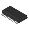
LM2575M-3.3
Texas Instruments
SWITCHING REGULATOR, VOLT-MODE
MLG1005S1N2ST000
TDK Corporation
FIXED IND 1.2NH 1A 100 MOHM SMD
MP3431GL-Z
Monolithic Power Systems Inc.
IC REG 16VOUT 21A HIGH EFFICIENC
CDRH6D28-150NC
Sumida America Components Inc.
FIXED IND 15UH 1.4A 84 MOHM SMD
GRM0225C1E9R1CDAEL
Murata Electronics
CAP CER 9.1PF 25V C0G/NP0 01005
BD180G
onsemi
TRANS PNP 80V 1A TO126
EP1M120F484C5
Intel
IC FPGA 303 I/O 484FBGA
0603YD474KAT2A
KYOCERA AVX
CAP CER 0.47UF 16V X5R 0603
MPQ2459GJ-AEC1-Z
Monolithic Power Systems Inc.
IC REG BUCK ADJ 500MA TSOT23-6
2N3637
Microchip Technology
TRANS PNP 175V 1A TO39
STP16CL596MTR
STMicroelectronics
IC LED DRIVER LINEAR 90MA 24SO
LTC1746CFW#PBF
Analog Devices Inc.
IC ADC 14BIT PIPELINED 48TSSOP
MMZ1608B601CTAH0
TDK Corporation
FERRITE BEAD 600 OHM 0603 1LN
ADP2303ARDZ-2.5-R7
Analog Devices Inc.
IC REG BUCK 2.5V 3A 8SOIC
ADT7467ARQ-REEL
onsemi
IC REMOTE THERMAL CTRLR 16-QSOP
AD633JN
Analog Devices Inc.
IC ANALOG MULTIPLIER 8-DIP
MC9S08SH4MTGR
NXP USA Inc.
IC MCU 8BIT 4KB FLASH 16TSSOP -

TC4421AVOA
Microchip Technology
IC GATE DRVR LOW-SIDE 8SOIC
VS-10WQ045FNTR-M3
Vishay General Semiconductor - Diodes Division
DIODE SCHOTTKY 45V 10A DPAK
PS2535L-1-F3-A
CEL
OPTOISOLATOR 5KV DARL 4SMD
PTV05020WAH
Texas Instruments
DC DC CONVERTER 0.8-3.6V
1N3328A
Solid State Inc.
DO5 50 WATT ZENER DIODES
R7F701A033AFP#KA8
Renesas Electronics America Inc
IC MCU 32BIT 144-LQFP
IRF7905TRPBF
Infineon Technologies
MOSFET 2N-CH 30V 7.8A/8.9A 8SO
LT1639IS
Analog Devices Inc.
IC OPAMP GP 4 CIRCUIT 14SO
OP284FSZ
Analog Devices Inc.
IC OPAMP GP 2 CIRCUIT 8SOIC
RG82865G
Intel
GRAPHICS AND MEMORY CONTROLLER H
UMK316B7225MLHT
Taiyo Yuden
CAP CER 2.2UF 50V X7R 1206
XCS30-3VQ100C
AMD
IC FPGA 77 I/O 100VQFP
TPS75515KC
Texas Instruments
IC REG LINEAR 1.5V 5A TO220-5
TPA0213DGQRG4
Texas Instruments
IC AMP CLASS AB MONO 2W 10MSOP
B39171B5070H810
Qualcomm (RF front-end (RFFE) filters)
FILTER SAW 167MHZ 10SMD
TS391SN2T1G
onsemi
IC COMPARATOR 1 GEN PUR 5TSOP
SN74LVC652APWR
Texas Instruments
IC TXRX NON-INVERT 3.6V 24TSSOP
SSCDANN060PGAA5
Honeywell Sensing and Productivity Solutions
SENSOR 60PSIG 0.19" 4.5V 8DIP -

MAX34406TETG+
Analog Devices Inc./Maxim Integrated
IC CURRENT SENSE 24TQFN
IR3473MTRPBF
Infineon Technologies
IC REG BUCK ADJUSTABLE 6A 16QFN
APX825A-46W6G-7
Diodes Incorporated
IC SUPERVISOR 1 CHANNEL SOT26
MCZ33904B5EK
NXP USA Inc.
IC INTERFACE SPECIALIZED 32SOIC
UMK107SD222JA-T
Taiyo Yuden
CAP CER 2200PF 50V 0603
PTZTE2543A
Rohm Semiconductor
DIODE ZENER 43V 1W PMDS
MAX8902BATA/V+T
Analog Devices Inc./Maxim Integrated
IC REG LIN POS ADJ 500MA 8TDFN
SBR3060CTFP
Diodes Incorporated
DIODE ARRAY SBR 60V 15A ITO220AB
170M5012
Eaton - Bussmann Electrical Division
FUSE SQUARE 630A 700VAC RECT
MC10H162P
onsemi
IC DECODER 1 X 3:8 16DIP
1N4005G
Good-Ark Semiconductor
RECTIFIER, GENERAL PURPOSE, GLAS
NJM2831F12-TE1
Nisshinbo Micro Devices Inc.
IC REG LINEAR 12V 100MA SOT23-5
PIC18LF458-I/P
Microchip Technology
IC MCU 8BIT 32KB FLASH 40DIP
LQP02TQ9N1H02D
Murata Electronics
FIXED IND 9.1NH 170MA 1.7OHM SMD
Z8018006PSG
Zilog
IC MPU Z180 6MHZ 64DIP
MAX627ESA+T
Analog Devices Inc./Maxim Integrated
IC GATE DRVR LOW-SIDE 8SOIC
IFS100B12N3E4_B39
Infineon Technologies
IGBT MOD 1200V 100A 515W
75869-104LF
Amphenol ICC (FCI)
CONN HEADER VERT 20POS 2.54MM